
With the popularity of smartphones, flat-panel TVs and other devices, the consumer electronics market has seen unprecedented growth. The ever-increasing competition has led the electronics manufacturing industry to place higher demands on product processes. Traditional processing methods have become increasingly unable to meet the needs of modern processes. Unstable product quality, melted parts, difficulty in forming normal nuclei, and low yield rates have become problems for manufacturers. The emergence of laser welding technology has played a major role in the production process of high-end electronic products, both in terms of product volume optimization as well as quality improvement.At present, laser welding in the electronics industry production is mainly used in the precision spot welding technology, precision spot welding technology has a small thermal deformation, the role of the area and location of precise control, high welding quality, the ability to achieve heterogeneous material welding, easy to achieve automation and other advantages, can be applied to electronic products in the shell, shield, USB connector, conductive patch, etc., but welding different materials, the need to use different welding methods . Follow GOLD MARK to learn more about the following.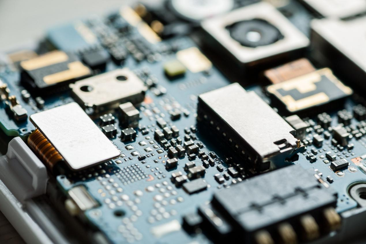 Laser precision spot welding method of high anti-materialWhen welding highly reflective materials such as aluminum and copper, different welding waveforms have a significant impact on the welding quality. Using a laser waveform with a front spike can break through the high reflectivity barrier. The instantaneous high peak power can quickly change the state of the metal surface and raise its temperature to the melting point, thus reducing the reflectivity of the metal surface and improving the energy utilization. In addition, since materials such as copper and aluminum conduct heat quickly, the appearance of the solder joint can be optimized by using a slow-drop waveform.On the other hand, the laser absorption rate of materials such as china, silver, copper and steel decreases with increasing wavelength, and for copper, the absorption rate of copper is close to 40% when the laser wavelength is 532 nm. Comparison of the characteristics of infrared laser and green laser shows that the infrared laser spot size is larger, the focal depth is short, and the absorption rate of copper is low; the green laser spot size is small, the focal depth is long, and the absorption rate of copper is high. The infrared laser and green laser pulse spot welding of copper, respectively, can be found that the infrared laser welding after the size of inconsistent welding joints, while the green laser welding joints size more uniform, consistent depth, smooth surface. The welding effect is more stable with the green laser, and the peak power required will be more than half of that of the infrared laser.
 Laser precision spot welding method for thin metal sheet materialsTraditional millisecond lasers are prone to penetration and large joints when welding thin sheet metal materials, while high inverse materials often have burst spots and false welds due to their own instability and low absorption of laser light in the solid state. In order to solve the thin plate and high inverse metal welding difficulties, through the fiber laser QCW / CW mode of analog and digital modulation, respectively, trigger once to achieve N pulse output, with less power to achieve a single point multi-pulse welding.Laser precision spot welding method for dissimilar materialsLaser welding of thin plate heterogeneous materials is highly susceptible to false welding, cracks, and low joint strength due to the large difference in physical properties, low mutual solubility, and the high probability of generating brittle compounds, which greatly reduce the mechanical properties of the weld head. The nanosecond laser with high beam quality is selected to suppress the formation of intermetallic compounds by high speed scanning method with precise control of heat input to realize the lap joint of thin plates of dissimilar metals and improve the weld formation and mechanical properties.Guangdong China cut CNC Machinery Co., Ltd. is a high-tech industry enterprise specialized in researching, manufacturing and selling the machines as follows: Laser Engraver, Fiber Laser Marking Machine, CNC Router. The products have been widely used in advertisement board, crafts and molding, architecture, seal, label, woodcutting and engraving, stonework decoration, leather cutting, garment industries, and so on. On the base of absorbing the international advanced technology, we provide the clients the most advanced production and perfect after-sale service. In recently years, our products have been sold not only in China, but also as far as Southeast Asia, Middle east, Europe, South America and other overseas Markets.Email: [email protected]
WeCha/WhatsApp: +868870255
Link to this article:Brief description of laser welding for different materials in the electronics industry
Reprint Statement: If there are no special instructions, all articles on this site are original. Please indicate the source for reprinting.:Cut Wiki,Thanks!^^